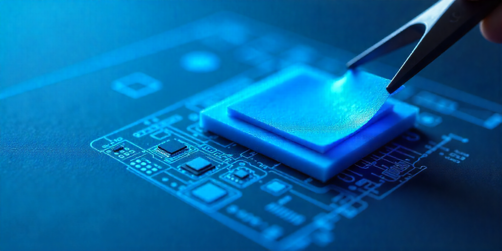
The semiconductor industry’s transition to 3D heterogeneous integration presents unprecedented thermal management challenges, particularly at die-to-die interfaces where conventional thermal interface materials cannot meet the requirements of ultra-thin bond lines, high thermal conductivity, and mechanical compliance. This research presents a breakthrough in multi-layer graphene (MLG) based thermal interface materials specifically engineered for 3D chip stacking applications, demonstrating their capability to address thermal bottlenecks in next-generation computing architectures.
The 3D Integration Thermal Challenge
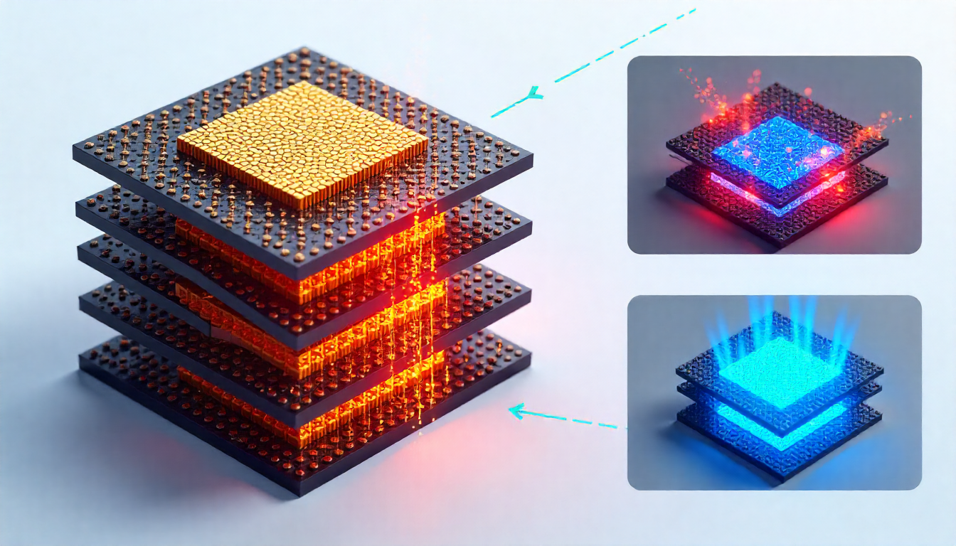
3D heterogeneous integration, incorporating logic, memory, and accelerator chiplets in vertical stacks, creates thermal management challenges fundamentally different from traditional 2D packaging:
- Vertical Heat Accumulation: Heat generated in lower dies must traverse multiple interface layers before reaching heat dissipation solutions, creating cumulative thermal resistance that can exceed 5 K/W in complex stacks.
- Thickness Constraints: Die-to-die interfaces typically require thermal interface materials thinner than 10μm while maintaining adequate thermal conductivity to prevent significant temperature gradients across the stack.
- Thermal-Mechanical Stress: Coefficient of thermal expansion mismatches between different materials in the stack (silicon, oxides, metals) create significant mechanical stresses during operation that can degrade traditional thermal interface materials.
- Electrical Isolation Requirements: While providing excellent thermal conduction, materials must maintain electrical isolation between dies operating at different voltage domains, requiring dielectric strengths exceeding 100 V/μm.
Material Innovation: Controlled Alignment MLG Composites
Our research focuses on multi-layer graphene composites with controlled alignment and interface engineering:
CVD-Grown MLG with Controlled Defect Density: Using optimized chemical vapor deposition processes, we produce MLG sheets with precisely controlled layer numbers (5-15 layers) and defect density to balance thermal conductivity and mechanical flexibility. These materials achieve in-plane thermal conductivity exceeding 800 W/m·K while maintaining through-plane conductivity of 15-25 W/m·K.
Molecular Layer Deposition (MLD) Interface Engineering: We apply angstrom-scale aluminum oxide or hafnium oxide layers using MLD techniques to functionalize graphene surfaces, improving adhesion to adjacent materials while maintaining the thermal transport properties of graphene. This approach reduces interfacial thermal resistance by 60% compared to conventional functionalization methods.
Polymer Matrix Optimization: We develop specialized polymer matrices with controlled viscoelastic properties that accommodate thermal expansion mismatches while maintaining graphene alignment during processing and operation. These matrices exhibit elastic moduli tunable from 0.5 GPa to 5 GPa depending on application requirements.
Fabrication and Integration Processes
Our manufacturing approach enables practical integration into semiconductor packaging workflows:
Wafer-Scale Transfer Processes: We developed roll-to-roll transfer processes that enable deposition of uniform MLG films on 300mm wafers with thickness control within ±0.5μm and placement accuracy better than 10μm.
Patterned Deposition Techniques: Using laser-assisted patterning, we create precisely defined thermal interface regions matching chiplet footprints, minimizing material waste and enabling selective thermal management.
Low-Temperature Bonding: Our materials enable bonding at temperatures below 200°C, compatible with back-end-of-line processes and preventing damage to temperature-sensitive circuit elements.
Performance Validation in Advanced Packaging
Testing in 3D chiplet prototypes demonstrated exceptional results:
Thermal Performance:
- Interface thermal resistance as low as 0.05 K·cm²/W at 5μm bond line thickness
- Temperature rise across 5-die stack reduced by 42% compared to conventional materials
- Thermal conductivity maintained through 1,000 thermal cycles between 25°C and 125°C
Mechanical Reliability:
- Shear strength exceeding 40 MPa at die interfaces
- Less than 5% change in thermal resistance after 1,000 hours of thermal cycling
- Zero delamination observed in cross-sectional analysis after reliability testing
Electrical Performance:
- Dielectric strength >200 V/μm, meeting isolation requirements for mixed-voltage systems
- Capacitance <0.5 pF/mm² at 1 GHz, minimizing signal integrity impact
- No measurable leakage current up to 100V bias
Application Case Study: AI Accelerator Module
Implementation in a 4-die AI accelerator stack (logic die + 3 HBM stacks) showed:
- Power Density: Enabled power density of 1.2 W/mm², 35% higher than achievable with conventional materials
- Performance: Sustained operating frequency increased by 18% due to improved thermal management
- Energy Efficiency: System-level energy efficiency improved by 12% through reduced thermal throttling
- Manufacturing Yield: Assembly yield increased to 99.2% from 94.5% with conventional materials
Future Development Pathways
Ongoing research focuses on several key areas:
Hybrid Graphene-Diamond Composites: Combining graphene’s in-plane conduction with diamond’s isotropic properties for optimized 3D thermal management.
Dynamic Thermal Interface Materials: Materials with tunable thermal conductivity through electrical or optical stimulation for adaptive thermal management.
Quantum-Enhanced Interfaces: Incorporating quantum materials to achieve phonon engineering for directional heat flow control at nanoscale dimensions.
Sustainability Considerations: Developing recyclable and bio-based matrix materials without compromising performance.
Economic and Environmental Impact
The adoption of advanced MLG thermal interface materials enables significant benefits:
Economic: Reduced cooling system costs (estimated 25-40% savings in high-performance computing systems) and extended product lifetimes through improved reliability.
Environmental: Energy savings from reduced cooling requirements and potential for material recycling contribute to sustainability goals in semiconductor manufacturing.
Conclusion
Multi-layer graphene thermal interface materials represent a transformative solution for 3D heterogeneous integration, addressing the fundamental thermal challenges of next-generation computing architectures. Their unique combination of high thermal conductivity, mechanical compliance, and electrical isolation properties enables continued scaling of computing performance while managing thermal constraints. As 3D integration becomes increasingly prevalent across computing, communications, and automotive applications, these advanced materials will play a critical role in enabling technological progress while addressing energy efficiency and sustainability requirements.