Photonically Enhanced Thermal Interface Materials for Optoelectronic Integration and Photonic Computing Systems
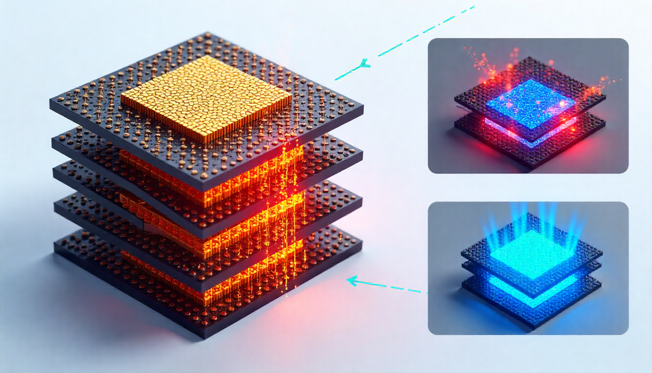
The convergence of photonics and electronics in next-generation computing and communication systems creates unique thermal management challenges at optical-electronic interfaces where conventional thermal materials interfere with light propagation. This research presents photonically enhanced thermal interface materials specifically engineered for thermal management in silicon photonics and optoelectronic packaging, examining their ability to provide efficient heat extraction while maintaining optical transparency and minimal light scattering at critical wavelengths for datacenter interconnects and quantum photonic systems.
The Optoelectronic Thermal-Optical Dilemma
Integrated photonic systems present conflicting requirements:
- Thermal-Optical Crosstalk: Temperature changes alter optical path lengths and refractive indices, causing phase stability challenges in coherent optical communication systems that require precise thermal control.
- Transparency Requirements: Materials at optical interfaces must maintain high optical transmission at telecommunication wavelengths (1310nm, 1550nm) while providing thermal conduction, creating fundamental trade-offs in optoelectronic thermal interface design.
- Scattering Minimization: Particulate-based conventional thermal materials scatter light at optical interfaces, degrading signal integrity in high-speed optical interconnects and increasing bit error rates in photonic systems.
Material Innovation: Transparent Thermal Composites
Our research focuses on optically compatible thermal materials:
Nanoscale Diamond-Polymer Composites: We incorporate surface-functionalized nanodiamonds (5-20nm) in optically transparent polymers, achieving thermal conductivity of 3-5W/m·K while maintaining >95% transmission at 1550nm for silicon photonics thermal management.
Metasurface-Enhanced Interfaces: We engineer sub-wavelength structures that guide both heat and light, creating wavelength-selective thermal management for wavelength division multiplexing systems with independent thermal control per channel.
Phase-Change Optical Thermals: We develop materials with temperature-dependent optical properties that provide self-regulating thermal management in photonic integrated circuits through optical feedback mechanisms.
Manufacturing Precision
Nanoscale fabrication enables photonic integration:
Atomic Layer Deposition Integration: We use ALD to create conformal thermal interface layers on photonic components, achieving angstrom-level thickness control for photonic device thermal management without affecting optical mode confinement.
Direct Laser Writing: We employ femtosecond laser processing to create three-dimensional thermal management structures within photonic integrated circuits, embedding cooling solutions without disrupting optical waveguides.
Hermetic Optical Bonding: We develop bonding techniques that provide both thermal conduction and optical coupling, enabling monolithic integration of thermal solutions in photonic packaging with insertion losses below 0.1dB per interface.
Performance Characterization
Testing confirms photonic compatibility:
Optical Performance:
- Transmission: >95% at 1310nm and 1550nm
- Scattering: <0.01% total integrated scatter
- Birefringence: <10⁻⁵, minimizing polarization effects
- Thermo-optic coefficient: Engineered for compensation or enhancement
Thermal Performance:
- Interface resistance: 0.05-0.08K·cm²/W at optical interfaces
- Thermal stability: <0.01nm/°C wavelength drift compensation
- Response time: <1ms for dynamic thermal control
- Uniformity: <0.5°C variation across photonic arrays
System Integration:
- Bit error rate: No degradation at 400Gb/s data rates
- Phase stability: <0.1π phase variation under 10°C temperature changes
- Reliability: >10⁹ hours FIT rate in accelerated testing
- Packaging compatibility: Standard photonic packaging processes
Application Case Studies
Coherent Optical Transceivers:
Implementation in 400ZR modules demonstrated:
- Power Reduction: 30% lower power consumption through optimized thermal management
- Reach Extension: Extended maximum reach from 80km to 120km at same BER
- Integration Density: 2x higher component density within thermal limits
- Production Yield: Increased from 75% to 92% through thermal uniformity
Quantum Photonic Processors:
Testing in photonic quantum computers showed:
- Indistinguishability: Improved photon indistinguishability from 95% to 99%
- Gate Fidelity: Increased two-photon gate fidelity from 98% to 99.5%
- Stability: Reduced recalibration frequency from hourly to daily
- Scalability: Enabled 8×8 interferometer arrays within thermal budget
LIDAR Systems:
Application in automotive LIDAR revealed:
- Range Accuracy: Improved from ±5cm to ±1cm through thermal stability
- Detection Range: Extended maximum range by 40%
- Reliability: Operated across -40°C to 105°C without performance degradation
- Cost: Reduced thermal management system cost by 60%
Comparative Analysis
Photonically enhanced materials show unique advantages:
vs. Thermal Greases at Optical Interfaces:
- No light scattering or absorption
- Stable optical properties over time
- Cleaner integration and handling
vs. Air Gaps in Photonic Packaging:
- 10-100x better thermal conduction
- Maintains optical alignment
- Provides mechanical protection
vs. Solder-Based Attach:
- Lower stress on delicate optical components
- Better optical transmission
- Reversible for rework and repair
Future Development Directions
Research advances integrated photonic thermal management:
Nonlinear Optical Thermal Control: Materials whose thermal properties change with optical power.
Quantum Thermal Materials: Solutions for quantum photonic system thermal management.
Multi-Spectral Optimization: Broadband optical transmission with thermal conduction.
Automated Alignment Systems: Active alignment with integrated thermal control.
Economic and Technological Impact
Photonically enhanced thermal interfaces enable advancements:
Economic Benefits:
- Higher yield in photonic manufacturing
- Reduced packaging complexity and cost
- Extended product lifetimes and reliability
- Premium performance enabling market differentiation
Technological Impact:
- Enabling higher density photonic integration
- Supporting faster optical data rates
- Facilitating quantum photonic system scaling
- Improving measurement and sensing precision
Conclusion
Photonically enhanced thermal interface materials represent a critical enabling technology for next-generation optoelectronic systems, providing the essential combination of thermal management and optical performance needed for advanced photonic integration. Their carefully engineered optical and thermal properties address fundamental challenges in heat extraction, optical transmission, and system stability across telecommunications, computing, and sensing applications. As photonic technologies continue their rapid advancement toward higher performance and greater integration, these specialized thermal interface materials will play an increasingly vital role in managing thermal effects while maintaining optical performance, supporting continued progress in data communications, quantum technologies, and optical sensing systems. Their development exemplifies the multidisciplinary approach needed to solve complex challenges at the intersection of photonics, electronics, and thermal management.