Low-Modulus, High-Conductivity Thermal Gap Fillers for Mitigating Thermomechanical Stress in Heterogeneous 2.5D and 3D Integrated Circuit Packages
The industry’s shift toward 2.5D and 3D integrated circuit (IC) packaging, combining multiple silicon dies, high-bandwidth memory (HBM), and interposers, introduces severe thermomechanical stress due to coefficient of thermal expansion (CTE) mismatch between dissimilar materials. This research presents a novel class of low-modulus, high-thermal-conductivity gap-filling materials engineered to dissipate heat and absorb stress in advanced heterogeneous semiconductor packaging. We examine how these materials simultaneously manage thermal hotspots and reduce warpage and interfacial delamination risks, thereby improving the yield, reliability, and performance of cutting-edge processors, accelerators, and system-in-package (SiP) modules.
The Thermomechanical Challenge in Advanced Packaging
The pursuit of higher performance through integration creates a multifaceted stress problem:
- Global Warpage and Die Stress: The assembly of large silicon dies, organic substrates, and copper pillars creates a complex stack with mismatched CTEs. During solder reflow (260°C) and operational cycling, this generates global package warpage and local die stress in 2.5D IC packages, leading to interconnect failures, keep-out zones, and assembly yield loss.
- Localized Hotspots and Thermal Crosstalk: In chiplets and 3D stacks, high-power compute dies are placed adjacent to or on top of sensitive components like HBM. Inadequate lateral heat spreading causes thermal interference between chiplets in heterogeneous integration, throttling performance and risking data corruption in memory.
- Underfill and Encapsulant Limitations: Traditional capillary underfills (CUF) and molded underfills (MUF) provide essential mechanical reinforcement but have poor thermal conductivity (~0.5 W/m·K). This creates a thermal bottleneck in the underfill region of high-power flip-chip packages, leaving heat trapped under the die.
Material Innovation: Decoupling Mechanical and Thermal Properties
We engineer materials that break the traditional trade-off between softness (for stress absorption) and thermal conductivity:
Dual-Network Polymer Matrix: We synthesize a hybrid polymer system with a rigid, highly cross-linked network for dimensional stability, interpenetrated by a soft, low-Tg (glass transition temperature) elastomeric network. This structure provides a persistently low elastic modulus (<1 MPa) over a wide temperature range from -55°C to 150°C, allowing it to continuously absorb stress during thermal cycling.
Hierarchical Filler Architecture for Percolation at Low Loading: Instead of relying on high filler loading (which increases modulus), we use a combination of large aspect-ratio boron nitride (BN) platelets and spherical alumina particles. The BN platelets form a thermally conductive percolation network at a low critical volume fraction, while the spheres prevent excessive viscosity rise. This achieves thermal conductivity >4 W/m·K at low modulus—a combination unattainable with conventional filled silicones.
Tailored Adhesion and Cohesion Balance: The material’s adhesion to various surfaces (silicon, SiO₂, SiN, mold compound) is carefully tuned to be strong enough to prevent delamination but weak enough to allow inelastic deformation at the interface, promoting stress decoupling in 3D stacked memory-on-logic packages. Its high cohesive strength prevents internal tearing.
Application Processes for Precision and Yield
The material is designed for manufacturability in high-precision semiconductor assembly:
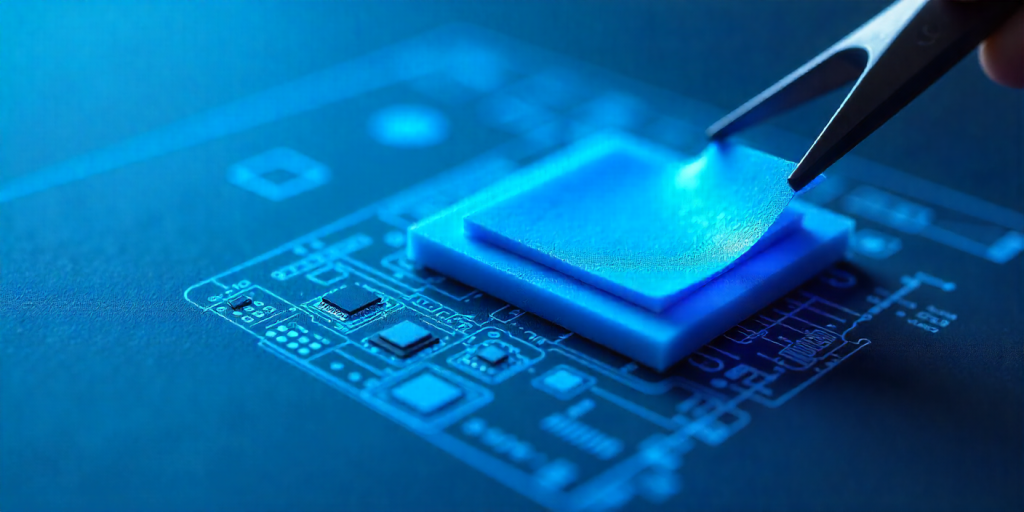
Dispensing for Complex Geometries: Formulated as a paste with tailored rheology (thixotropy), it can be precisely dispensed around tall, dense copper pillar arrays and into the narrow gaps between stacked dies, ensuring complete void-free filling in high-aspect-ratio package gaps.
Curing Compatibility: It undergoes a low-stress curing process (either thermal or UV) that minimizes additional shrinkage stress on the delicate package structure, compatible with downstream processes like molding and ball attach.
Non-Conductive and Ion-Free: The formulation is strictly non-conductive and uses ultra-pure, ion-free ingredients to prevent electromigration and corrosion in fine-pitch micro-bump interconnections.
Validation in Leading-Edge Product Platforms
Testing in qualification vehicles and early product integration demonstrates comprehensive benefits:
Mechanical Stress Mitigation:
- Warpage Reduction: Reduced maximum package warpage during the reflow profile by >40% compared to packages using standard thermal interface materials or no stress buffer.
- Interconnect Reliability: In thermal cycling tests (-55°C to 125°C), packages with the advanced gap filler showed a 10x reduction in micro-bump fatigue failures after 1,000 cycles.
- Die Crack Prevention: Absorbed stress from global bending, effectively eliminating die cracking in large, thin dies (e.g., >800 mm² reticle sizes).
Thermal Performance Enhancement:
- Junction Temperature (Tj) Reduction: By providing an efficient lateral heat spreading path away from the compute die, the material lowered the Tj of adjacent HBM stacks by 15-20°C under full bandwidth operation.
- Hotspot Mitigation: Reduced the peak temperature gradient across a large CPU die by over 30%, enabling more uniform performance and higher sustainable clock speeds.
- System-Level Cooling: By efficiently transferring heat from the die stack to the package lid or integrated heat spreader (IHS), it improved the overall effectiveness of the external cooling solution.
Future Development: Toward Multifunctional Integration
The research roadmap focuses on adding functionality to the stress-managing thermal matrix:
Electrically Insulating but Thermally Anisotropic: Developing versions with enhanced in-plane thermal conductivity (>10 W/m·K) for better lateral spreading while maintaining through-plane electrical insulation for thermal management of adjacent power delivery and signal routing layers.
Integrated Sensing: Exploring the incorporation of dielectric or resistive additives that change properties with temperature or strain, enabling embedded health monitoring for predictive maintenance of advanced IC packages.
Conclusion: A Foundational Material for the 3D Integration Era
Low-modulus, high-conductivity thermal gap fillers represent a pivotal material innovation for the semiconductor industry’s journey into 3D integration. By simultaneously addressing the dual, often competing, challenges of thermomechanical stress and heat dissipation, they directly enable the reliable and high-performance packaging of heterogeneous systems. This material class is not merely an incremental improvement but a necessary enabler, allowing packaging engineers to push the boundaries of interconnect density, die size, and power delivery without being limited by warpage, cracking, or thermal crosstalk. As the industry continues to embrace chiplets and 3D stacking to extend Moore’s Law, these advanced interfacial materials will be essential for turning complex electrical designs into robust, manufacturable, and high-performance physical products.