Micro-Scale Thermal Interfaces: Cooling Next-Gen 3D Chip Stacks
The relentless drive toward higher performance and efficiency has led semiconductor design into the third dimension. 3D chip stacking, heterogeneous integration, and chiplet-based architectures offer tremendous benefits but create unprecedented thermal challenges. Heat must now be managed not just from the top surface of a single die, but from multiple vertically stacked dies, through silicon interposers, and across intricate chiplet assemblies. This evolution demands a new class of micro-scale thermal interface materials specifically engineered for the unique requirements of advanced semiconductor packaging and 3D integration.
Thermal Challenges in 3D and Heterogeneous Architectures
Modern packaging approaches introduce several thermal bottlenecks:
- Vertical Heat Accumulation: In 3D stacks, heat from lower dies must pass through upper dies to reach the heatsink, creating thermal coupling between vertically adjacent chips that can limit performance of the entire stack.
- Material Compatibility Constraints: TIMs used in through-silicon via (TSV) structures and micro-bump arrays must have coefficient of thermal expansion matching both silicon and the interconnect materials to prevent thermo-mechanical stress failure in chip stacks.
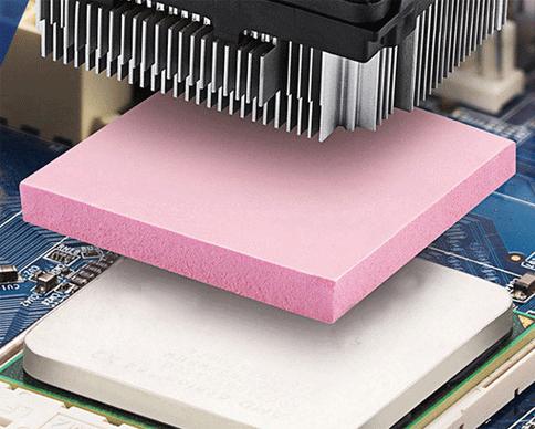
- Ultra-Thin Interface Requirements: The vertical distance between dies in 3D stacks can be less than 100 micrometers, requiring TIMs that deliver high performance in layers as thin as 10-50 microns for die-to-die interfaces.
- Non-Uniform Heat Distribution: Chiplet architectures create localized hot spots at chiplet boundaries and interconnect regions where thermal management is particularly challenging.
Advanced Material Solutions for Chip-Scale Cooling
Innovations in material science are addressing these microscopic challenges:
- Atomic Layer Deposited (ALD) TIMs: These ultra-thin, conformal coatings applied at the atomic scale provide exceptional thermal interface performance for nanoscale gaps in 3D chip stacks. ALD materials can achieve thermal boundary conductance exceeding 100 MW/m²K, dramatically reducing resistance at critical interfaces.
- Metal-Infiltrated Polymer Composites: By infiltrating polymer matrices with metal nanowires or liquid metal droplets, researchers have created materials that combine the compliance of polymers with thermal conductivities approaching pure metals—ideal for stress-tolerant interfaces in chiplet assemblies.
- Graphene and 2D Material Laminates: Vertically aligned graphene films offer extremely high through-plane thermal conductivity while maintaining electrical insulation, making them perfect for thermal management in silicon interposer applications.
- Phase Change Materials with Nanoscale Features: Advanced PCMs incorporating nanoparticles or nanostructured surfaces enhance thermal performance at micro-scale thicknesses while maintaining compliance to accommodate packaging warpage and die tilt.
Integration Techniques and Manufacturing Considerations
Successfully implementing micro-scale TIMs requires specialized processes:
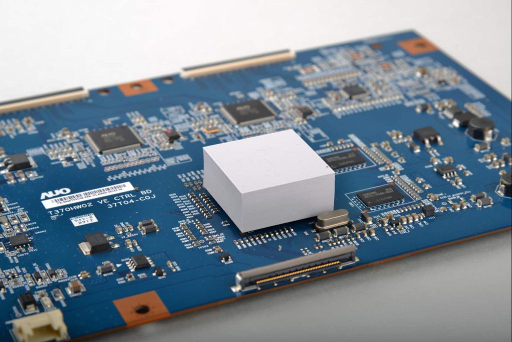
- Wafer-Level Application: Many advanced TIMs are now applied at the wafer level before dicing, enabling high-volume, cost-effective thermal interface integration in semiconductor manufacturing.
- Precision Dispensing and Patterning: Inkjet printing and micro-dispensing technologies allow precise placement of different TIM formulations on specific areas of a chip or interposer, enabling graded thermal interface designs that optimize performance across varied thermal environments.
- Thermal Compression Bonding Integration: Advanced TIMs are increasingly designed to function as both thermal interface and bonding material in hybrid bonding processes, simplifying assembly while improving thermal and mechanical performance.
- In-Situ Cure and Processing: Some materials require specialized curing under vacuum or controlled atmosphere to achieve optimal properties, necessitating integration with advanced packaging equipment.
Performance Characterization and Reliability Testing
Evaluating micro-scale TIMs presents unique measurement challenges:
- Nanoscale Thermal Mapping: Techniques like time-domain thermoreflectance and scanning thermal microscopy are essential for characterizing thermal performance at the length scales relevant to 3D packaging.
- Interfacial Stress Analysis: Micro-Raman spectroscopy and X-ray microdiffraction help evaluate thermo-mechanical stresses at TIM interfaces, critical for predicting reliability in chip stacks.
- Accelerated Aging Tests: Specialized test structures and protocols simulate long-term operation of 3D integrated circuits to validate TIM performance over product lifetimes.
- Thermal Cycling Endurance: Materials must withstand the extreme thermal gradients present in vertically stacked architectures through thousands of power cycles.
Applications Across Computing Segments
Different computing domains are driving specific micro-scale TIM developments:
- High-Performance Computing: CPU-GPU memory stacks in exascale systems require TIMs that can manage heat fluxes exceeding 500 W/cm² while maintaining structural integrity through thermal cycling.
- Artificial Intelligence Accelerators: 3D memory-on-logic configurations in AI chips demand TIMs with exceptional performance in thin layers between memory and processing elements.
- Mobile and Edge Devices: Heterogeneous chiplet packages in smartphones need TIMs that provide effective cooling while adding minimal thickness and weight.
- Automotive Electronics: Multi-die power modules for electric vehicles require TIMs that maintain performance across automotive temperature ranges while withstanding vibration and thermal shock.
Future Directions and Research Frontiers
Several emerging areas promise further advances:
- Quantum-Dot Enhanced Interfaces: Materials incorporating thermally conductive quantum dots that provide phonon matching between dissimilar materials, reducing interfacial thermal resistance.
- Self-Assembled Monolayer TIMs: Molecular-scale interfacial layers that optimize thermal transport across material boundaries through precise chemical bonding.
- Dynamic Reconfiguration: Materials that can change their thermal transport properties in response to electrical or thermal signals, enabling adaptive cooling within 3D stacks.
- Integrated Thermal Sensors: TIMs with embedded nanoscale temperature sensors providing real-time thermal mapping of chip stacks for intelligent thermal management.
The development of micro-scale thermal interface technologies is enabling the continued advancement of semiconductor packaging and 3D integration. By solving thermal challenges at the chip scale, these materials are helping unlock the performance benefits of advanced architectures while ensuring reliability and manufacturability—key requirements for the next generation of computing systems.