Thermal Putty vs. Pad: When to Use Each for Electronics
Faced with an uneven surface or components of different heights? Both thermal putty and gap pads are designed to conform, but they have distinct behaviors. Choosing wrong can lead to poor cooling or a mess. Here’s a clear breakdown to help you decide.
Direct Comparison: Workability and Performance
| Feature | Thermal Putty | Thermal Gap Pad |
|---|---|---|
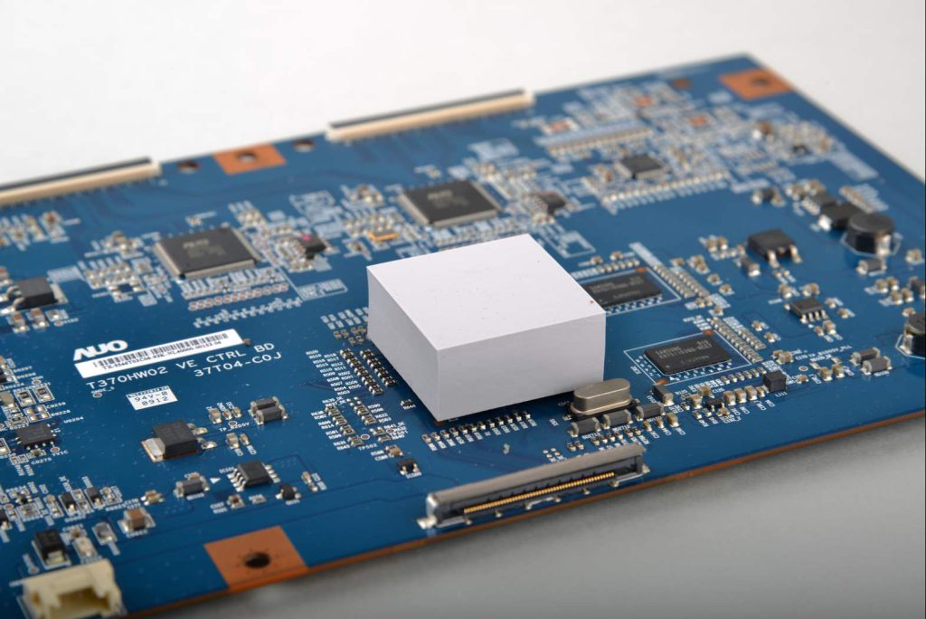
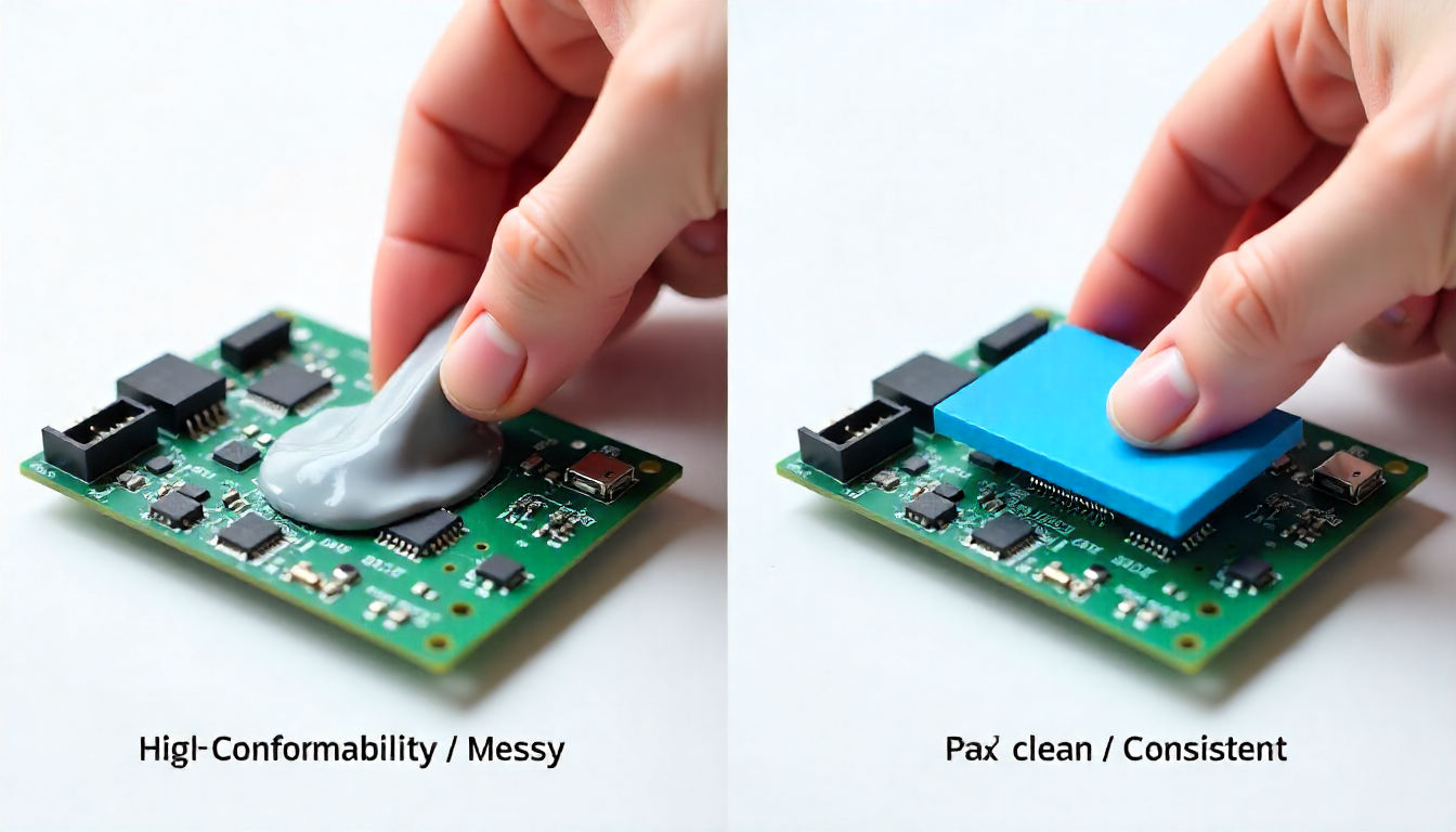
| Form & Handling | Clay-like, moldable by hand. Can be messy. | Pre-formed solid sheet. Clean and easy to cut. |
| Best For | Extreme height variations, irregular 3D shapes, and prototyping. | Planar surfaces, consistent gaps, and high-volume production. |
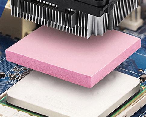
| Conformability | Exceptional. Will fill any void it’s pressed into. | Good, but limited by its thickness and hardness (durometer). |
| Pressure Sensitivity | Low. Conforms under very light pressure. | Requires significant compressive force for optimal thinning. |
| Reusability | Generally not reusable once compressed. | Can often be repositioned if not torn. |
| Cleanup | Can leave oily residue; harder to clean. | Typically cleaner; may leave slight silicone oil film. |
When to Reach for Thermal Putty:
- You have components with a >1mm height difference on the same plane.
- The surface is curved or highly irregular.
- You are in a prototyping or repair phase and need a one-size-fits-all solution for various gaps.
When a Gap Pad is the Better Choice:
- You have many identical assemblies in production (consistency is key).
- The gap is relatively uniform and you can specify a precise thickness.
- You require UL94 flammability ratings or specific material certifications that putty may not have.
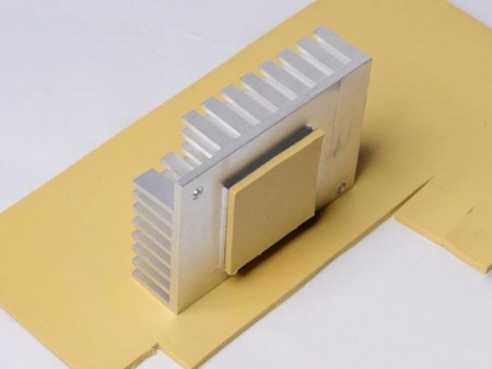
Pro Tip: For challenging applications, a hybrid approach can work: use a gap pad for the main chip, and a dab of putty for a single tall adjacent component.
Understanding this fundamental choice saves time, cost, and ensures your components run cool and reliably.