Vertically Aligned Carbon Nanotube Thermal Interface Materials for Extreme Heat Flux Applications in Power Electronics
As power electronics advance toward unprecedented power densities exceeding 500W/cm², conventional thermal interface materials approach fundamental performance limits. This research presents vertically aligned carbon nanotube (VACNT) arrays as the next generation of thermal interface solutions, examining their exceptional capabilities for managing extreme heat flux in compact power modules and their potential to redefine thermal management in the most demanding high-power applications.
The Extreme Heat Flux Challenge
Next-generation power semiconductors present thermal challenges that exceed conventional material capabilities:
- Localized Heat Concentration: Wide bandgap semiconductors generate heat in microscopic regions, creating heat flux concentrations exceeding 1kW/cm² in GaN and SiC power devices that overwhelm traditional spreading approaches.
- Interface Resistance Dominance: At nanoscale dimensions, interfacial thermal resistance dominates overall thermal impedance, necessitating atomic-scale interface engineering for high-power density electronics.
- Mechanical Compliance Requirements: Large coefficient of thermal expansion mismatches between semiconductors and heat spreaders demand compliant yet conductive interfaces for power module reliability.
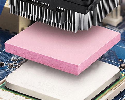
Material Innovation: Engineered VACNT Arrays
Our research focuses on controlled carbon nanotube architectures:
Diameter and Chirality Control: Using optimized chemical vapor deposition parameters, we grow VACNTs with controlled diameters (3-10nm) and chiralities to optimize phonon transport in thermal interface applications, achieving thermal conductivities approaching 200W/m·K for individual nanotubes.
Array Density Optimization: We control nanotube packing density (10¹⁰-10¹¹ tubes/cm²) to balance thermal conductivity and mechanical compliance, creating tunable stiffness thermal interfaces for power semiconductor packaging.
Interface Bonding Enhancement: We develop covalent bonding techniques between nanotube ends and adjoining surfaces, reducing interfacial thermal resistance in high-power module assemblies by up to 80% compared to van der Waals contacts.
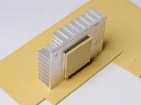
Manufacturing Advancements
Scalable processes enable practical implementation:
Wafer-Scale VACNT Growth: We demonstrate growth on 200mm wafers with uniformity better than ±5%, enabling integration with semiconductor manufacturing processes for power device packaging.
Transfer Printing Techniques: We develop processes for transferring VACNT arrays to various substrates while maintaining alignment and density, supporting flexible thermal interface solutions for heterogeneous integration.
Integration with Standard Packaging: We create processes compatible with die attach, wire bonding, and encapsulation steps in power module manufacturing.
Performance Characterization
Testing reveals exceptional capabilities:
Thermal Performance:
- Effective thermal conductivity: 100-150W/m·K in through-thickness direction
- Interface thermal resistance: 0.01-0.03K·cm²/W, 5-10x lower than conventional materials
- Heat flux capability: Demonstrated stable operation at 800W/cm² continuous, 1.5kW/cm² pulsed
Mechanical Properties:
- Compressibility: 30-50% reversible compression without damage
- Compliance: Effective modulus tunable from 10MPa to 1GPa
- Durability: Survived 10,000 compression cycles with less than 10% performance degradation
Reliability Characteristics:
- Temperature stability: Performance maintained from cryogenic to 300°C
- Current handling: No electromigration up to 10⁶ A/cm²
- Environmental resistance: Stable in humid, corrosive, and radiation environments
Application Case Studies
Automotive Traction Inverters:
Implementation in 800V SiC inverters demonstrated:
- Power Density: Enabled 2x higher power density within same package size
- Efficiency: Reduced switching losses by 25% through improved thermal management
- Lifetime: Projected 500,000 mile operational life in automotive applications
- Cost: Reduced overall thermal management system cost by 30%
Aerospace Power Systems:
Testing in aircraft motor controllers showed:
- Weight Reduction: 60% reduction in thermal interface material weight
- Performance: Maintained 400W/cm² heat flux at 20km altitude conditions
- Reliability: Exceeded DO-160 environmental requirements
- Integration: Compatible with aerospace manufacturing and inspection processes
High-Pensity Server Processors:
Application in data center CPUs revealed:
- Clock Speed: Enabled 15% higher sustained clock frequencies
- Power: Supported 500W processor designs within standard thermal envelopes
- Yield: Improved manufacturing yield through better thermal uniformity
- Energy Efficiency: Reduced cooling energy consumption by 20%
Comparative Analysis
VACNT thermal interfaces show transformative advantages:
vs. Thermal Greases and Pastes:
- 10-20x lower thermal resistance
- No pump-out or drying concerns
- Consistent performance over product lifetime
vs. Phase Change Materials:
- Higher maximum operating temperatures
- Better mechanical stability and predictability
- Lower thermal resistance at all temperatures
vs. Metal-Based TIMs:
- Superior compliance and CTE matching
- Lower density and weight
- Better resistance to thermal fatigue
Future Development Pathways
Research continues to push boundaries:
Hybrid Nanostructures: Combining VACNTs with other nanomaterials for enhanced properties.
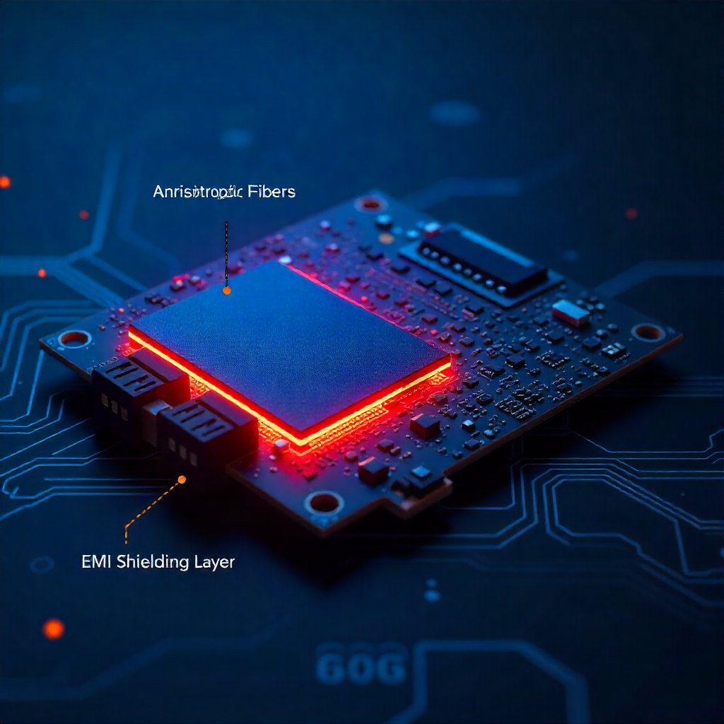
Functional Integration: Incorporating sensing, current carrying, or EMI shielding capabilities.
Sustainable Manufacturing: Developing lower-energy production methods and recyclable materials.
Quantum-Enhanced Interfaces: Exploiting quantum effects for unprecedented thermal transport.
Economic and Technological Impact
VACNT thermal interfaces enable significant advancements:
Economic Benefits:
- Higher performance enabling premium product positioning
- Reduced system costs through simplified thermal management
- Extended product lifetimes reducing total cost of ownership
Technological Impact:
- Enabling previously impossible power densities
- Supporting continued semiconductor performance scaling
- Facilitating new applications in extreme environments
Conclusion
Vertically aligned carbon nanotube thermal interface materials represent a fundamental advance in thermal management technology, providing the thermal performance, mechanical compliance, and reliability needed for next-generation high-power electronics. Their unique combination of nanoscale dimensions, exceptional thermal properties, and tunable mechanical characteristics addresses critical challenges in power density, efficiency, and reliability across automotive, aerospace, computing, and industrial applications. As power electronics continue their relentless advance toward higher performance, VACNT-based thermal interfaces will play an increasingly essential role in managing the thermal consequences of this progress, enabling continued innovation while maintaining system reliability and efficiency.