When Proximity is the Problem: TIM-Induced Impedance Shifts in High-Speed Digital Circuits
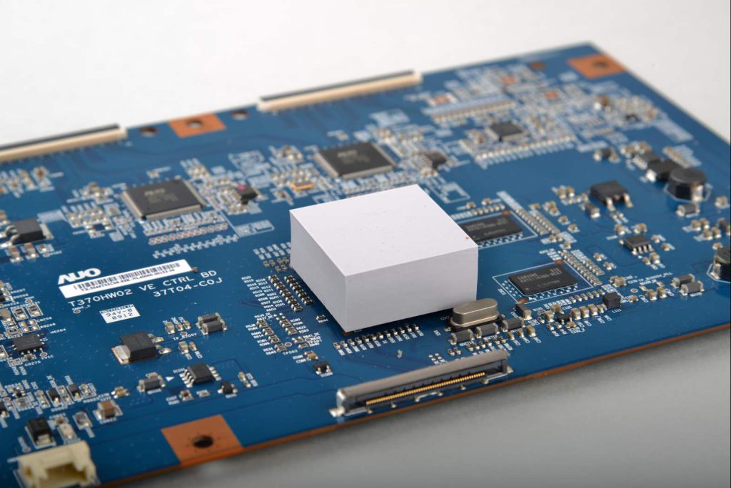
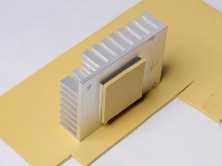
In the race for miniaturization and higher clock speeds, thermal management structures are placed millimeters away from multi-gigabit-per-second data lanes. The Thermal Interface Material, typically viewed as an electrically insulating bystander, now becomes an integral part of the local dielectric environment, capable of degrading signal integrity if ignored.
The Mechanism: Localized Effective Dielectric Constant (Dk)
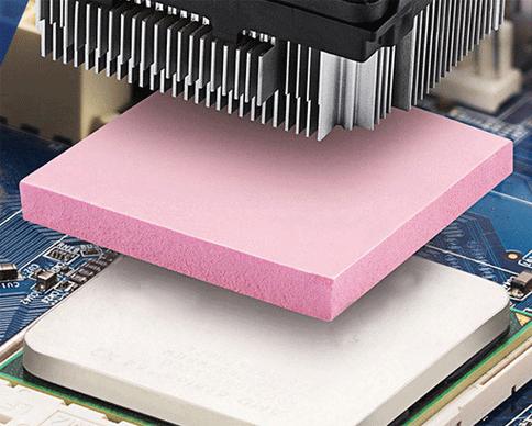
The impedance of a PCB trace is a function of its geometry and the effective Dk of the surrounding material. When a TIM with a different Dk than air (Dk=1) or the PCB substrate (e.g., FR4 Dk~4) is placed directly above or beside a trace, it changes this local effective Dk.
- Problem: A TIM with a high and/or variable Dk (some silicones can have Dk > 4) will lower the trace impedance and increase capacitance, potentially causing impedance mismatches, increased insertion loss, and slower edge rates. This can manifest as eye diagram closure and bit errors.
Mitigation Strategies for High-Speed Design:
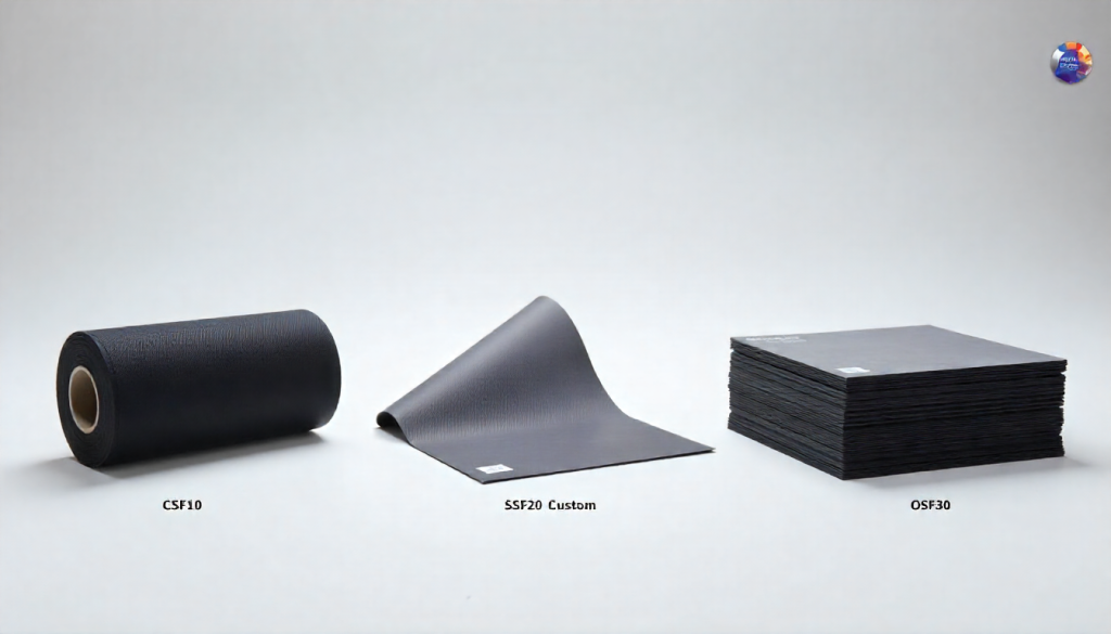
- Material Selection for Low Dk: For applications where TIM must overlap signal areas, specify materials with a low, stable, and well-documented dielectric constant. Certain polyolefin-based or engineered foam materials can offer favorable Dk properties.
- Strategic Keep-Out Zones: The most reliable method is to establish clearance rules in your PCB layout. Define keep-out zones around high-speed traces where no TIM (or other high-Dk material) can encroach. This requires close collaboration between thermal and SI engineers from the start.
- 3D Electromagnetic Simulation: For mission-critical interfaces (e.g., > 25 Gbps), use 3D EM simulation tools to model the exact geometry, including the TIM’s presence. This allows you to quantify the impact and adjust trace geometry (e.g., slightly narrow the trace under the TIM area) to compensate for the impedance shift.
Ignoring the TIM in your signal integrity model is a growing risk. By treating the TIM as a defined material layer in your stack-up and simulations, you can prevent subtle, system-level performance issues that are notoriously difficult to debug post-production.